 English▼


products categories
- Battery Production Equipment Line
- Battery Lab Pilot Equipment Line
- Lithium Battery Pack Assembly Line
- Solid State Battery Assembly Line
- Sodium Ion Battery Production Line
- Supercapacitor Assembly Line
- Lithium Ion Battery Recycling Plant
- Dry Electrode Preparation Solution
- Perovskite Based Solar Cell Lab Line
- Li ion Battery Materials
- Cathode Active Materials
- Anode Active Materials
- Customized Battery Electrode
- Coin Cell Parts
- Lithium Chip
- Cylindrical Cell Parts
- Battery Current Collectors
- Battery Conductive Materials
- Electrolyte
- Metal Mesh
- Battery Binder
- Separator and Tape
- Aluminum Laminate Film
- Nickel Strip
- Battery Tabs
- Graphene Materials
- Nickel Felt
- Titanium Fiber Felt
- Battery
- Battery Pack Machine & Compoments
- Battery Pack Compoments
- Turnkey Solutions Battery Pack Assembly Line
- Cell Sorter
- Battery Pack Spot Welder
- Laser Welder
- Battery Charging Discharging Tester
- Battery Pack Aging Machine
- Battery Pack Comprehensive Tester
- CCD Visual Inspector
- Battery Pape Sticking Machine
- BMS Testing Machine
- Al Wire Bonding Machine
- Lithium Battery Machine
- Battery Tester & Analyzer
- Battery Safety Tester
- Material Characterization Tester
- Rolling Press Machine
- Spot Welding Machine
- Vacuum Mixer Machine
- Crimping/Disassembling Machine
- Vacuum Sealing Machine
- Electrolyte Filling
- Stacking/Winding Machine
- Electrode Cutter/Slitter
- Pouch Forming Machine
- NMP Solvent Treatment System
- Lithium Battery Production Plant
- Vacuum Glove Box
- Furnaces
- Coaters
- PVD Coater
- Laboratory Press Machine
- Large Press Machine
- Planetary Centrifugal Mixer
- Ball Mill
- Laboratory Machine
- Cutting Machine
- Metal Foam
contact us
- If you have questions, please contact us, all questions will be answered
- WhatsApp : +86 18659217588
- Email : David@tmaxcn.com
- Email : Davidtmaxcn@gmail.com
- Add : No. 39, Xinchang Road, Xinyang, Haicang Dist., Xiamen, Fujian, China (Mainland)
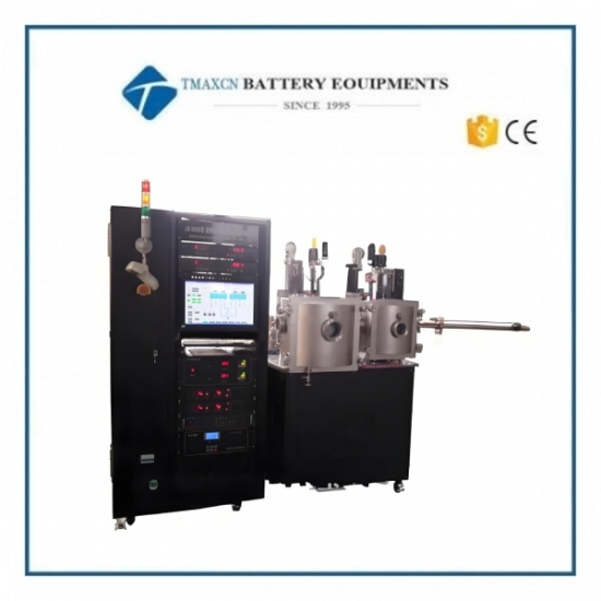
Double Chamber PVD Coater System For Thin Film Deposition Preparation
Model Number:
TMAX-PC-JS12Input Power:
2000WCompliance:
CE CertifiedWarranty:
One Year limited warranty with lifetime supportShipping Port:
XiamenMOQ:
1Payment:
L/C D/A D/P T/T Western UnionDelivery Time:
5 days
- WhatsApp : +86 18659217588
- Email : David@tmaxcn.com
- Email : Davidtmaxcn@gmail.com
- Wechat : 18659217588
Previous:
Multi-Material Deposition Magnetron Sputter Coating System Equipment For Organic MultilayerNext:
Nano PVD Magnetron Sputtering System For Metals, Alloys, Dielectric, Perovskite Films
Double Chamber PVD Coater System For Thin Film Deposition Preparation
Model: TMAX-PC-JS12-With Ion Source Cleaning & Assisted Sputtering
General Information
Category |
Description |
Application |
Preparation of nanoscale monolayer/multilayer functional films (hard coatings, metallic/semiconductor/dielectric films). Suitable for research labs, universities, and small-batch production. |
Key Features |
• Anode-layer ion source (cleaning + assisted deposition) • Reverse sputtering for adhesion enhancement • Automated PC-controlled process |
System Structure |
Sputtering chamber, 3 magnetron targets, heating stage, DC/RF power supplies, gas/pumping systems, vacuum measurement, control unit. |
Technical Parameters
Parameter |
Specification |
Chamber Design |
Vertical front-loading, stainless steel construction |
Base Vacuum |
≤5×10⁻⁵ Pa (sputtering chamber) |
Pumping Speed |
Recovers to 5×10⁻⁴ Pa in 100 min (via bypass valve + turbopump) |
Leak Rate |
≤5×10⁻⁷ Pa·L/s |
Pressure Rise Rate |
≤10 Pa after 12 hours (power off) |
Pumping System |
Domestic turbomolecular pump + mechanical pump |
Targets |
3 × 3-inch HV targets (2 standard, 1 strong magnetic field) |
Power Supplies |
• RF: 600 W, 13.56 MHz (auto-matching) • DC: 2 × 1000 W |
Target-to-Sample Distance |
40–120 mm (adjustable) |
Substrate Heating |
Max 450°C, programmable (rate/dwell time controllable) |
Film Thickness Uniformity |
±5% (e.g., Cu/Al: 4–5 μm; Ni/PTFE: 1–2 μm over 2-inch area) |
Adhesion Strength |
Survives 3 tape-peeling tests (glass/Si/ceramic) |
Pre-Cleaning |
Reverse sputtering + anode-layer ion source |
Gas Control |
2 MFCs (Ar + reactive gases), MKS-brand, mixing enabled |
Baking |
IR heating, max 150°C |
Safety |
Water/power failure interlocks, anti-misoperation protection |
Automation |
PC-controlled (target switching, substrate rotation, temperature) |
Performance Advantages & Suitability
Feature |
Benefit |
Target Applications |
Ion Source + Sputtering |
Ensures clean surfaces and high adhesion |
Semiconductor films, optical coatings |
Multi-Mode Deposition |
Supports DC/RF, reactive sputtering, multilayers |
Research on novel functional materials |
Precise Automation |
Reduces human error, improves reproducibility |
Small-batch prototyping, academic labs |
Rapid Pumping |
Minimizes downtime between runs |
High-throughput R&D environments |
Key Features & Suitability
· High-Precision Deposition: Ensures uniform, high-adhesion films for research and prototyping.
· Multi-Functional Cleaning: Combines ion source + reverse sputtering for optimal surface preparation.
· Flexible Configuration: Supports DC/RF modes, multilayer films, and reactive sputtering.
· User-Friendly Automation: PC-controlled workflow reduces manual errors.
Ideal for: Advanced material research, semiconductor labs, and functional coating development requiring reproducible, high-quality thin films.


 +86 13174506016
 David@tmaxcn.com

