 English▼


products categories
- Battery Production Equipment Line
- Battery Lab Pilot Equipment Line
- Lithium Battery Pack Assembly Line
- Solid State Battery Assembly Line
- Sodium Ion Battery Production Line
- Supercapacitor Assembly Line
- Lithium Ion Battery Recycling Plant
- Dry Electrode Preparation Solution
- Perovskite Based Solar Cell Lab Line
- Li ion Battery Materials
- Cathode Active Materials
- Anode Active Materials
- Customized Battery Electrode
- Coin Cell Parts
- Lithium Chip
- Cylindrical Cell Parts
- Battery Current Collectors
- Battery Conductive Materials
- Electrolyte
- Metal Mesh
- Battery Binder
- Separator and Tape
- Aluminum Laminate Film
- Nickel Strip
- Battery Tabs
- Graphene Materials
- Nickel Felt
- Titanium Fiber Felt
- Battery
- Battery Pack Machine & Compoments
- Battery Pack Compoments
- Turnkey Solutions Battery Pack Assembly Line
- Cell Sorter
- Battery Pack Spot Welder
- Laser Welder
- Battery Charging Discharging Tester
- Battery Pack Aging Machine
- Battery Pack Comprehensive Tester
- CCD Visual Inspector
- Battery Pape Sticking Machine
- BMS Testing Machine
- Al Wire Bonding Machine
- Lithium Battery Machine
- Battery Tester & Analyzer
- Battery Safety Tester
- Material Characterization Tester
- Rolling Press Machine
- Spot Welding Machine
- Vacuum Mixer Machine
- Crimping/Disassembling Machine
- Vacuum Sealing Machine
- Electrolyte Filling
- Stacking/Winding Machine
- Electrode Cutter/Slitter
- Pouch Forming Machine
- NMP Solvent Treatment System
- Lithium Battery Production Plant
- Vacuum Glove Box
- Furnaces
- Coaters
- PVD Coater
- Laboratory Press Machine
- Large Press Machine
- Planetary Centrifugal Mixer
- Ball Mill
- Laboratory Machine
- Cutting Machine
- Metal Foam
contact us
- If you have questions, please contact us, all questions will be answered
- WhatsApp : +86 18659217588
- Email : David@tmaxcn.com
- Email : Davidtmaxcn@gmail.com
- Add : No. 39, Xinchang Road, Xinyang, Haicang Dist., Xiamen, Fujian, China (Mainland)
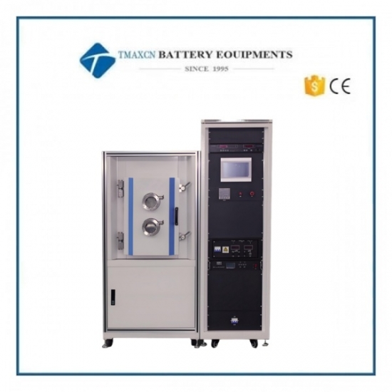
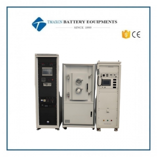
Electron Beam Evaporation Coating System For Layer Deposition In OLED, Solar Cell & Semiconductor
Model Number:
TMAX-TK-DZ02Input Power:
2000WCompliance:
CE CertifiedWarranty:
One Year limited warranty with lifetime supportShipping Port:
XiamenMOQ:
1Payment:
L/C D/A D/P T/T Western UnionDelivery Time:
5 days
- WhatsApp : +86 18659217588
- Email : David@tmaxcn.com
- Email : Davidtmaxcn@gmail.com
- Wechat : 18659217588
Electron Beam Evaporation Coating System For Layer Deposition In OLED, Solar Cell & Semiconductor
TMAX-TK-DZ02-Precision Thin-Film Deposition Solution for Research & Industry
1. Product Overview
The TMAX-TK-DZ02 is a high-performance electron beam evaporation system designed for advanced thin-film research and small-batch production. Featuring a compact vertical design with semi-automatic controls, it offers exceptional film uniformity and material versatility for both academic and industrial applications.
2. Key Features & Advantages
2.1 Precision Deposition Performance
· Achieves ≤±5% film thickness uniformity via rotating substrate holder (0-40 rpm)
· Ultra-high vacuum (6.0×10⁻⁵ Pa) ensures minimal contamination
· Fast pumping system reaches working vacuum in ≤30 minutes
2.2 Advanced Configuration Options
· 8kW E-gun with 6-crucible carousel (domestic/import options)
· Optional Kaufman ion source for improved film density and adhesion
· Triple resistive evaporation sources for low-temperature materials
2.3 User-Oriented Design
· PLC + touchscreen control for reproducible processes
· Compact footprint (2.5×1.6m) ideal for laboratory environments
· Comprehensive safety protection system (cooling/voltage/pressure monitoring)
3. Technical Specifications
Parameter |
Specification |
Chamber Design |
Vertical cylinder, side-opening |
Chamber Dimensions |
Φ500 × H650 mm |
Base Pressure |
≤6.0×10⁻⁵ Pa |
Pumping Speed |
2000 L/s |
Heating Temperature |
RT - 300°C (substrate) |
Substrate Stage |
Φ200 mm rotating (max Φ300 mm loading) |
Film Uniformity |
≤±5% |
E-Gun Power |
8 kW |
Control System |
PLC + Touchscreen |
Total Power Consumption |
≥17 kW |
4. Application Areas
4.1 Optical Coatings
· Anti-reflection coatings
· Laser optics
· IR filters and mirrors
4.2 Electronics & Semiconductors
· Conductive films (Au, ITO)
· Dielectric layers (SiO₂, Al₂O₃)
· Semiconductor device fabrication
4.3 Functional Materials
· Ferroelectric films (PZT)
· MEMS and sensor coatings
· Wear/corrosion resistant layers
5. Technical Highlights
5.1 Multi-Material Deposition
· Processes metals (Al, Au, Ti), oxides (SiO₂), and organic films
· Handles both low-vapor-pressure and refractory materials
5.2 Research-Grade Flexibility
· Supports multi-layer deposition for complex structures
· Substrate heating enables optimized film crystallization
5.3 Production-Ready Reliability
· Robust mechanical design for continuous operation
· Low maintenance requirements with easy consumable replacement
6. Why Choose?
· Academic/Industrial Versatility: From basic research to pilot production
· Cost Efficiency: Lower operational costs than comparable systems
· Future Expandability: Modular design accepts process upgrades


 +86 13174506016
 David@tmaxcn.com

