 English▼


products categories
- Battery Production Equipment Line
- Battery Lab Pilot Equipment Line
- Lithium Battery Pack Assembly Line
- Solid State Battery Assembly Line
- Sodium Ion Battery Production Line
- Supercapacitor Assembly Line
- Lithium Ion Battery Recycling Plant
- Dry Electrode Preparation Solution
- Perovskite Based Solar Cell Lab Line
- Li ion Battery Materials
- Cathode Active Materials
- Anode Active Materials
- Customized Battery Electrode
- Coin Cell Parts
- Lithium Chip
- Cylindrical Cell Parts
- Battery Current Collectors
- Battery Conductive Materials
- Electrolyte
- Metal Mesh
- Battery Binder
- Separator and Tape
- Aluminum Laminate Film
- Nickel Strip
- Battery Tabs
- Graphene Materials
- Nickel Felt
- Titanium Fiber Felt
- Battery
- Battery Pack Machine & Compoments
- Battery Pack Compoments
- Turnkey Solutions Battery Pack Assembly Line
- Cell Sorter
- Battery Pack Spot Welder
- Laser Welder
- Battery Charging Discharging Tester
- Battery Pack Aging Machine
- Battery Pack Comprehensive Tester
- CCD Visual Inspector
- Battery Pape Sticking Machine
- BMS Testing Machine
- Al Wire Bonding Machine
- Lithium Battery Machine
- Battery Tester & Analyzer
- Battery Safety Tester
- Material Characterization Tester
- Rolling Press Machine
- Spot Welding Machine
- Vacuum Mixer Machine
- Crimping/Disassembling Machine
- Vacuum Sealing Machine
- Electrolyte Filling
- Stacking/Winding Machine
- Electrode Cutter/Slitter
- Pouch Forming Machine
- NMP Solvent Treatment System
- Lithium Battery Production Plant
- Vacuum Glove Box
- Furnaces
- Coaters
- PVD Coater
- Laboratory Press Machine
- Large Press Machine
- Planetary Centrifugal Mixer
- Ball Mill
- Laboratory Machine
- Cutting Machine
- Metal Foam
contact us
- If you have questions, please contact us, all questions will be answered
- WhatsApp : +86 18659217588
- Email : David@tmaxcn.com
- Email : Davidtmaxcn@gmail.com
- Add : No. 39, Xinchang Road, Xinyang, Haicang Dist., Xiamen, Fujian, China (Mainland)
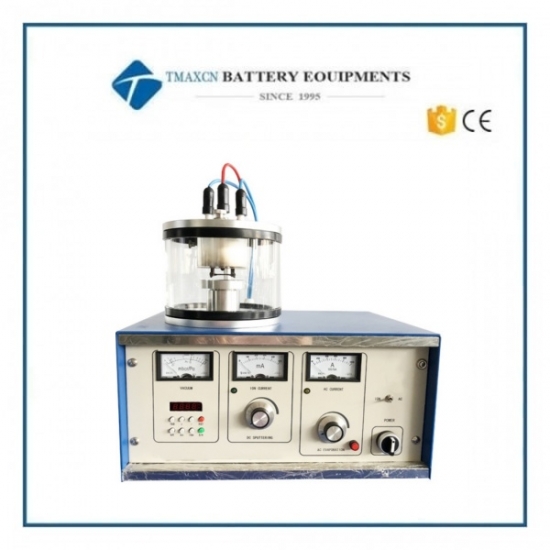
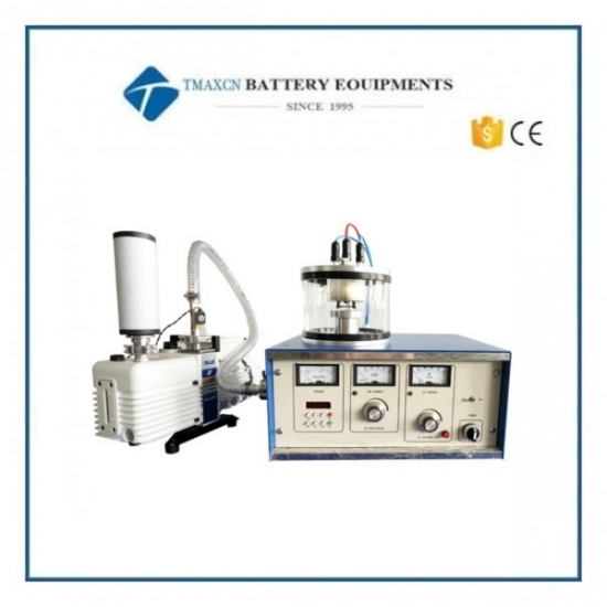
Lab Ion Sputtering & Evaporation PVD Coater Machine for SEM for Glove Box
Model Number:
TMAX-BY-ZDInput Power:
2000WCompliance:
CE CertifiedWarranty:
One Year limited warranty with lifetime supportShipping Port:
XiamenMOQ:
1Payment:
L/C D/A D/P T/T Western UnionDelivery Time:
5 days
- WhatsApp : +86 18659217588
- Email : David@tmaxcn.com
- Email : Davidtmaxcn@gmail.com
- Wechat : 18659217588
Lab Ion Sputtering & Evaporation PVD Coater Machine for SEM for Glove Box
TMAX-BY-JS03- Ion Sputtering & Evaporation Coater for SEM
Specification
Integrated with sputtering and thermal evaporation functions, this compact and user-friendly instrument is designed for high-quality thin-film deposition, particularly for SEM sample preparation. It supports multiple metal targets for sputtering and carbon fiber evaporation, offering precise control over coating parameters.
Technical Specifications
Parameter |
Value |
Dimensions |
305 mm × 400 mm × 390 mm (W×D×H) |
Vacuum Chamber Material |
Borosilicate glass, 160 mm × 110 mm (D×H) |
Target (Upper Electrode) |
50 mm × 0.1 mm (D×H) |
Sputtering Targets |
Au (standard), optional Ag, Pt, etc. |
Target Size |
φ50 mm |
Sample Stage |
Compatible with 50 mm/70 mm diameter; customizable |
Sputtering Voltage |
0–1600 V (DC), adjustable |
Sputtering Current |
0–50 mA |
Sputtering Timer |
0–360 s |
Carbon Evaporation Current |
0–100 A (AC) |
Evaporation Material |
Carbon fiber |
Evaporation Voltage |
0–30 V |
Evaporation Time |
0–1 s |
Gas Inlet Valve |
Compatible with φ3 mm tubing |
Process Gases |
Multiple options |
Power Supply |
220 V (110 V optional), 50 Hz |
Vacuum Pump |
2L rotary vane pump (VRD-8, domestic) |
Key Features
1. Dual-Function Design
·Combines ion sputtering (Au, Pt, Ag, Cu, etc.) and thermal evaporation (carbon fiber) for versatile applications.
·Ideal for high-resolution microscopy (SEM, TEM, EBSD) requiring ultra-fine carbon films (<1 nm).
2. Precision Control
·Adjustable sputtering current, vacuum pressure, and gas selection to optimize coating rate and particle size.
·Digital timer for reproducible processes.
3. Enhanced Sample Protection
·Conductive coatings eliminate charging effects in non-conductive samples.
·Carbon films protect beam-sensitive materials (e.g., biological/plastic samples) from electron beam damage.
4. Efficiency & Reliability
·Compact footprint with automated vacuum protection to prevent short circuits.
·Uniform film deposition with short processing time.
Applications
· Electron Beam-Sensitive Samples (e.g., polymers, biological tissues): Coating mitigates structural damage.
· Non-Conductive Materials: Metal layers (Au, Pt) dissipate charge, improving SEM imaging.
· Advanced Materials: Enhances conductivity and surface analysis (EBSD, microprobe) for semiconductors/composites.


 +86 13174506016
 David@tmaxcn.com

