 English▼


products categories
- Battery Production Equipment Line
- Battery Lab Pilot Equipment Line
- Lithium Battery Pack Assembly Line
- Solid State Battery Assembly Line
- Sodium Ion Battery Production Line
- Supercapacitor Assembly Line
- Lithium Ion Battery Recycling Plant
- Dry Electrode Preparation Solution
- Perovskite Based Solar Cell Lab Line
- Li ion Battery Materials
- Cathode Active Materials
- Anode Active Materials
- Customized Battery Electrode
- Coin Cell Parts
- Lithium Chip
- Cylindrical Cell Parts
- Battery Current Collectors
- Battery Conductive Materials
- Electrolyte
- Metal Mesh
- Battery Binder
- Separator and Tape
- Aluminum Laminate Film
- Nickel Strip
- Battery Tabs
- Graphene Materials
- Nickel Felt
- Titanium Fiber Felt
- Battery
- Battery Pack Machine & Compoments
- Battery Pack Compoments
- Turnkey Solutions Battery Pack Assembly Line
- Cell Sorter
- Battery Pack Spot Welder
- Laser Welder
- Battery Charging Discharging Tester
- Battery Pack Aging Machine
- Battery Pack Comprehensive Tester
- CCD Visual Inspector
- Battery Pape Sticking Machine
- BMS Testing Machine
- Al Wire Bonding Machine
- Lithium Battery Machine
- Battery Tester & Analyzer
- Battery Safety Tester
- Material Characterization Tester
- Rolling Press Machine
- Spot Welding Machine
- Vacuum Mixer Machine
- Crimping/Disassembling Machine
- Vacuum Sealing Machine
- Electrolyte Filling
- Stacking/Winding Machine
- Electrode Cutter/Slitter
- Pouch Forming Machine
- NMP Solvent Treatment System
- Lithium Battery Production Plant
- Vacuum Glove Box
- Furnaces
- Coaters
- PVD Coater
- Laboratory Press Machine
- Large Press Machine
- Planetary Centrifugal Mixer
- Ball Mill
- Laboratory Machine
- Cutting Machine
- Metal Foam
contact us
- If you have questions, please contact us, all questions will be answered
- WhatsApp : +86 18659217588
- Email : David@tmaxcn.com
- Email : Davidtmaxcn@gmail.com
- Add : No. 39, Xinchang Road, Xinyang, Haicang Dist., Xiamen, Fujian, China (Mainland)
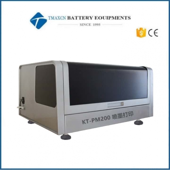
Printing Area 297mm×210mm Mini Ink Jet Printer Equipment Used in Perovskite Solar Cell
Model Number:
TMAX-KT-PM200Compliance:
CE CertifiedWarranty:
One year limited warranty with lifetime technical supportPlace of Origin:
ChinaPayment:
L/C D/A D/P T/T Western UnionDelivery Time:
5 days
- WhatsApp : +86 18659217588
- Email : David@tmaxcn.com
- Email : Davidtmaxcn@gmail.com
- Wechat : 18659217588
Printing Area 297mm×210mm Mini Ink Jet Printer Equipment Used in Perovskite Solar Cell

A. Product introduction:
Inkjet printer has been applied in the field of perovskite solar cells due to its features such as high material utilization rate, low cost, high process efficiency, patternability, and large-area fabrication. In the preparation methods of perovskite solar cells, the small-area perovskite solar cells fabricated based on inkjet printing technology have achieved an efficiency close to 20%, with the highest reaching 22.7%. While the perovskite solar cells manufactured by traditional solution spin coating method have an average efficiency of around 16% and the highest efficiency is 19.4%. Therefore, the inkjet printing technology for manufacturing perovskite solar cells has gained popularity in terms of conversion efficiency. Inkjet printing also has advantages such as high uniformity of the formed film and good film formation properties. It can be applied to materials in various directions, including solvents, water-based, and UV. The application fields include printed electronics, flexible electronics, organic electronics and bioelectronics, etc. It can be used for printing and manufacturing various microelectronic circuits, RF antennas, 5G antennas, sensors, electric heating electrodes, etc., and can also print test OLED ink, TFE ink and quantum dot ink, etc. for touch screens and OLED/QLED lighting display fields.
B. Product features:
a.Piezoelectric waveform: Open waveform control software
b.The edge trimming and thinning function balances the ink diffusion
c.Negative pressure adsorption and heating platform
d.Single nozzle with dual channels, with 192 spray holes in each channel
e.The printing platform adsorbs and heats the substrate
f.The minimum printing line width and line spacing are 50-75 μ m
g.The single-print thickness range of the material is 20-200nm (adjustable freely).
h.Support graphic pixel pre-trimming edges
i.It can be combined with near-infrared nanophotonics sintering
j.It can be equipped with heating for the inner channel of the nozzle
k.Independent 4 nozzles
l.Visual CCD alignment and registration
m.Multi-material parallel and serial printing
n.3pl small ink dots, open waveform
o.2400dpi high-precision printing
p.UV curing module
C. Technical specifications:
Parameters |
Indicator |
Motion axis |
Three axes, X,Y,Z |
Printing platform |
Negative pressure adsorption, heated |
Print size: X*Y |
297mm*210mm |
Print height Z |
0~10mm |
Mechanical repeatability accuracy |
0.02 mm |
Number of nozzles |
Standard configuration: 2 (supports 4) |
Ink droplet size |
Minimum 3.0pl |
Ink type |
Compatible with water-based, solvent and UV ink |
Printing accuracy |
0.075mm to 0.1mm |
Ink supply principle |
Four independent negative pressure ink supply systems |
Ink stack module |
Four sets of independent ink stacks, moisturizing |
Supported format |
1-bit TIF, DXF,Gerber *, 3D slice files stl, 3mf, 3ds, etc. (*DXF,Gerber formats are provided with RIP software) |
Resolution |
1200*1200, 2400*2400 |
Curing lamp |
365nm UV curing lamp |
Power supply/power |
220V/50Hz, 1.5kw |
External dimensions |
960mm(L)x709mm(W)x618mm(H) |
Equipment working environment |
Temperature: +20℃ to +30℃ Relative humidity: 40% to 60% |
Application |
Preparation of electrode circuits, OLeds, solar cells, sensors, semiconductors and other devices |
Optoelectronic device preparation |
Including perovskite, graphene, carbon nanotubes, OLED/QLED, OPV, OTFT, quantum dot ink, sensors, TFE packaging, PI printing film, bank inkjet printing, etc. |


 +86 13174506016
 David@tmaxcn.com

