 English▼


products categories
- Battery Production Equipment Line
- Battery Lab Pilot Equipment Line
- Lithium Battery Pack Assembly Line
- Solid State Battery Assembly Line
- Sodium Ion Battery Production Line
- Supercapacitor Assembly Line
- Lithium Ion Battery Recycling Plant
- Dry Electrode Preparation Solution
- Perovskite Based Solar Cell Lab Line
- Li ion Battery Materials
- Cathode Active Materials
- Anode Active Materials
- Customized Battery Electrode
- Coin Cell Parts
- Lithium Chip
- Cylindrical Cell Parts
- Battery Current Collectors
- Battery Conductive Materials
- Electrolyte
- Metal Mesh
- Battery Binder
- Separator and Tape
- Aluminum Laminate Film
- Nickel Strip
- Battery Tabs
- Graphene Materials
- Nickel Felt
- Titanium Fiber Felt
- Battery
- Battery Pack Machine & Compoments
- Battery Pack Compoments
- Turnkey Solutions Battery Pack Assembly Line
- Cell Sorter
- Battery Pack Spot Welder
- Laser Welder
- Battery Charging Discharging Tester
- Battery Pack Aging Machine
- Battery Pack Comprehensive Tester
- CCD Visual Inspector
- Battery Pape Sticking Machine
- BMS Testing Machine
- Al Wire Bonding Machine
- Lithium Battery Machine
- Battery Tester & Analyzer
- Battery Safety Tester
- Material Characterization Tester
- Rolling Press Machine
- Spot Welding Machine
- Vacuum Mixer Machine
- Crimping/Disassembling Machine
- Vacuum Sealing Machine
- Electrolyte Filling
- Stacking/Winding Machine
- Electrode Cutter/Slitter
- Pouch Forming Machine
- NMP Solvent Treatment System
- Lithium Battery Production Plant
- Vacuum Glove Box
- Furnaces
- Coaters
- PVD Coater
- Laboratory Press Machine
- Large Press Machine
- Planetary Centrifugal Mixer
- Ball Mill
- Laboratory Machine
- Cutting Machine
- Metal Foam
contact us
- If you have questions, please contact us, all questions will be answered
- WhatsApp : +86 18659217588
- Email : David@tmaxcn.com
- Email : Davidtmaxcn@gmail.com
- Add : No. 39, Xinchang Road, Xinyang, Haicang Dist., Xiamen, Fujian, China (Mainland)
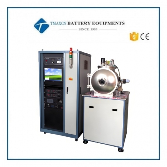
Auto Magnetron Sputtering Deposition System For Metals, Perovskite, Semiconductors, MEMS
Model Number:
TMAX-PC-JS09Input Power:
2000WCompliance:
CE CertifiedWarranty:
One Year limited warranty with lifetime supportShipping Port:
XiamenMOQ:
1Payment:
L/C D/A D/P T/T Western UnionDelivery Time:
5 days
- WhatsApp : +86 18659217588
- Email : David@tmaxcn.com
- Email : Davidtmaxcn@gmail.com
- Wechat : 18659217588
Previous:
Multi-target Magnetron Sputtering Machine For Parylene,OLED, Solar Cell & SemiconductorNext:
Dual-Target Magnetron Sputtering Coating System For Perovskite & Solar Cell Film
Auto Magnetron Sputtering Deposition System For Metals, Perovskite, Semiconductors, MEMS
Model: TMAX-PC-JS09-Multi-target, Multi-film Deposition
1. Specifications
Parameter |
Specification |
Chamber Design |
Single-chamber, vertical front-loading (stainless steel/vacuum-grade materials) |
Base Vacuum |
≤5×10⁻⁵ Pa |
Pump-down Time |
100 min (to ≤5×10⁻⁴ Pa after N2 venting) |
Leak Rate |
≤5×10⁻⁷ Pa·L/s |
Magnetron Targets |
3 × 3-inch (2 standard-field, 1 high-field, DC/RF compatible, Kurt J. Lesker) |
Power Supplies |
1 × RF (600 W, 13.56 MHz), 2 × DC (1000 W, AE Corp.) |
Substrate Stage |
3-position, rotating (5–30 RPM), heated (up to 450°C), bias voltage (1000 V) |
Target-Substrate Distance |
40–120 mm (80–120 mm with ion source) |
Gas Control |
2-channel MKS mass flow controllers (Ar + reactive gases) |
Film Thickness Uniformity |
≤5% on 2-inch area (Cu/Al: 4–5 µm, Ni/PTFE: 1–2 µm) |
Adhesion Test |
Passes 3× tape test (glass, Si, ceramic substrates) |
Additional Features |
Reverse sputtering, anode-layer ion source, safety interlocks, computer control |
2. Key Features & Benefits
· Uniform films with ≤5% thickness variation, ideal for research and prototyping.
· Multi-layer capability (e.g., Al/Ni, Al/PTFE) with automated target switching.
✔ Advanced Process Control
· Computer-controlled deposition (temperature, rotation, gas flow).
· Ion-assisted deposition enhances film density and adhesion.
✔ Flexible & Reliable Design
· Three-target system supports diverse materials (metals, dielectrics, semiconductors).
· Substrate heating (450°C) and rotation ensure high-quality coatings.
✔ Research-Optimized Safety
· Fail-safe protections (water/power interlocks, anti-misoperation).
· Controlled environment with bake-out and contamination liners.
3. Ideal Applications
· Academic & Industrial R&D: Thin-film studies, optoelectronics, protective coatings.
· Semiconductor & MEMS: Precise metal/dielectric layers for device fabrication.
· Advanced Materials: Hard coatings (e.g., tooling), functional films (e.g., PTFE).
4. Why Choose This System?
· Repeatable results with automated workflows.
· Imported critical components (Kurt J. Lesker targets, AE power supplies) ensure reliability.
· Compact footprint with full-featured capabilities for labs.


 +86 13174506016
 David@tmaxcn.com

