 English▼


products categories
- Battery Production Equipment Line
- Battery Lab Pilot Equipment Line
- Lithium Battery Pack Assembly Line
- Solid State Battery Assembly Line
- Sodium Ion Battery Production Line
- Supercapacitor Assembly Line
- Lithium Ion Battery Recycling Plant
- Dry Electrode Preparation Solution
- Perovskite Based Solar Cell Lab Line
- Li ion Battery Materials
- Cathode Active Materials
- Anode Active Materials
- Customized Battery Electrode
- Coin Cell Parts
- Lithium Chip
- Cylindrical Cell Parts
- Battery Current Collectors
- Battery Conductive Materials
- Electrolyte
- Metal Mesh
- Battery Binder
- Separator and Tape
- Aluminum Laminate Film
- Nickel Strip
- Battery Tabs
- Graphene Materials
- Nickel Felt
- Titanium Fiber Felt
- Battery
- Battery Pack Machine & Compoments
- Battery Pack Compoments
- Turnkey Solutions Battery Pack Assembly Line
- Cell Sorter
- Battery Pack Spot Welder
- Laser Welder
- Battery Charging Discharging Tester
- Battery Pack Aging Machine
- Battery Pack Comprehensive Tester
- CCD Visual Inspector
- Battery Pape Sticking Machine
- BMS Testing Machine
- Al Wire Bonding Machine
- Lithium Battery Machine
- Battery Tester & Analyzer
- Battery Safety Tester
- Material Characterization Tester
- Rolling Press Machine
- Spot Welding Machine
- Vacuum Mixer Machine
- Crimping/Disassembling Machine
- Vacuum Sealing Machine
- Electrolyte Filling
- Stacking/Winding Machine
- Electrode Cutter/Slitter
- Pouch Forming Machine
- NMP Solvent Treatment System
- Lithium Battery Production Plant
- Vacuum Glove Box
- Furnaces
- Coaters
- PVD Coater
- Laboratory Press Machine
- Large Press Machine
- Planetary Centrifugal Mixer
- Ball Mill
- Laboratory Machine
- Cutting Machine
- Metal Foam
contact us
- If you have questions, please contact us, all questions will be answered
- WhatsApp : +86 18659217588
- Email : David@tmaxcn.com
- Email : Davidtmaxcn@gmail.com
- Add : No. 39, Xinchang Road, Xinyang, Haicang Dist., Xiamen, Fujian, China (Mainland)
-
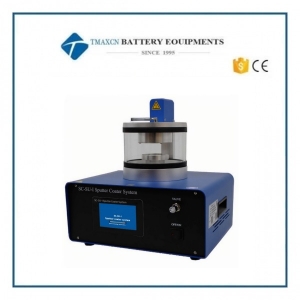 PVD Magnetron Sputtering System For Thin Film Deposition In Research, Semiconductor Prototyping and Optical Coating
PVD Magnetron Sputtering System For Thin Film Deposition In Research, Semiconductor Prototyping and Optical Coating Model: Lith-SD-JS02-Sputtering System for Research Labs, Semiconductor Prototyping, and Optical Coating Product Overview The Plasma Magnetron Sputtering System (Model: TMAX-SD-JS02) is a compact, user-friendly instrument designed for high-quality thin film deposition. With a quartz chamber (150 × 120 mm) and a maximum sputtering rate of 8 nm/min, it is ideal for research and small-scale production requiring precise, uniform coatings. Compatible with inert gases (Ar, N₂) and versatile metal targets (Au, Ag, Pt, etc.), this system combines efficiency with advanced operational features. Technical Specifications Parameter Specification Quartz Chamber Size 150 × 120 mm Sample Stage Size 70 mm (diameter) Sputtering Area 50 mm (diameter) Max. Vacuum Degree 5 Pa Process Gases Argon, Nitrogen (flow rate adjustable) Max. Sputtering Rate 8 nm/min Power Consumption 200 W Dimensions (W×D×H) 360 × 310 × 150 mm Operating Temperature 0–40°C Relative Humidity < 85% Installation Horizontal desktop placement Key Features & Advantages 1. Intuitive Control & Monitoring 4.3" color touchscreen with graphical interface for real-time display of sputtering current, voltage, and vacuum levels. 2. Flexible Gas & Target Options Adjustable inert gas flow (Ar/N₂) and support for 50 mm diameter metal targets (1–2 mm thickness), enabling quick material swaps and process reproducibility. 3. Modular & User-Centric Design ·Split-type quartz chamber for easy maintenance. ·Height-adjustable sample stage (±20 mm) with rotational alignment. ·Auto-venting post-sputtering simplifies sample handling. 4. Compact & Reliable ·Space-saving footprint with multi-layered software protections for extended durability. 5. Uniform Film Quality ·Dense, homogeneous coatings compatible with noble and transition metals (Au, Ag, Pt, etc.). Target Applications · Research Labs: Thin film studies, surface engineering, and material science. · Semiconductor Prototyping: Deposition of conductive/metallic layers. · Optics & Electronics: Functional coatings for sensors or display components. Note: Optimized for small substrates (≤50 mm) and low-to-medium throughput requirements. html {margin:0;padding:0;} body {margin:0;padding:5px;} body, td {font:12px/1.5 "sans serif",tahoma,verdana,helvetica;} body, p, div {word-wrap: break-word;} p {margin:5px 0;} table {border-collapse:collapse;} img {border:0;} noscript {display:none;} table.ke-zeroborder td {border:1px dotted #AAA;} img.ke-flash { border:1px solid #AAA; background-image:url(https://www.lithmachine.com/js/htmledit/kindeditor/themes/common/flash.gif); background-position:center center; background-repeat:no-repeat; width:100px; height:100px; } img.ke-rm { border:1px solid #AAA; background-image:url(https://www.lithmachine.com/js/htmledit/kindeditor/themes/common/rm.gif); background-position:center center; background-repeat:no-repeat; width:100px; height:100px; } img.ke-media { border:1px solid #AAA; background-image:url(https://www.lithmachine.com/js/htmledit/kindeditor/themes/common/media.gif); background-position:center center; background-repeat:no-repeat; width:100px; height:100px; } img.ke-anchor { border:1px dashed #666; width:16px; height:16px; } .ke-script, .ke-noscript, .ke-display-none { display:none; font-size:0; width:0; height:0; } .ke-pagebreak { border:1px dotted #AAA; font-size:0; height:2px; } html {margin:0;padding:0;} body {margin:0;padding:5px;} body, td {font:12px/1.5 "sans serif",tahoma,verdana,helvetica;} body, p, div {word-wrap: break-word;} p {margin:5px 0;} table {border-collapse:collapse;} img {border:0;} noscript {display:none;} table.ke-zeroborder td {border:1px dotted #AAA;} img.ke-flash { border:1px solid #AAA; background-image:url(https://www.lithmachine.com/js/htmledit/kindeditor/themes/common/flash.gif); background-position:center center; background-repeat:no-repeat; width:100px; height:100px; } img.ke-rm { border:1px solid #AAA; background-image:url(https://www.lithmachine.com/js/htmledit/kindeditor/themes/common/rm.gif); background-position:center center; background-repeat:no-repeat; width:100px; height:100px; } img.ke-media { border:1px solid #AAA; background-image:url(https://www.lithmachine.com/js/htmledit/kindeditor/themes/common/media.gif); background-position:center center; background-repeat:no-repeat; width:100px; height:100px; } img.ke-anchor { border:1px dashed #666; width:16px; height:16px; } .ke-script, .ke-noscript, .ke-display-none { display:none; font-size:0; width:0; height:0; } .ke-pagebreak { border:1px dotted #AAA; font-size:0; height:2px; }
 +86 13174506016
 David@tmaxcn.com

