 English▼


products categories
- Battery Production Equipment Line
- Battery Lab Pilot Equipment Line
- Lithium Battery Pack Assembly Line
- Solid State Battery Assembly Line
- Sodium Ion Battery Production Line
- Supercapacitor Assembly Line
- Lithium Ion Battery Recycling Plant
- Dry Electrode Preparation Solution
- Perovskite Based Solar Cell Lab Line
- Li ion Battery Materials
- Cathode Active Materials
- Anode Active Materials
- Customized Battery Electrode
- Coin Cell Parts
- Lithium Chip
- Cylindrical Cell Parts
- Battery Current Collectors
- Battery Conductive Materials
- Electrolyte
- Metal Mesh
- Battery Binder
- Separator and Tape
- Aluminum Laminate Film
- Nickel Strip
- Battery Tabs
- Graphene Materials
- Nickel Felt
- Titanium Fiber Felt
- Battery
- Battery Pack Machine & Compoments
- Battery Pack Compoments
- Turnkey Solutions Battery Pack Assembly Line
- Cell Sorter
- Battery Pack Spot Welder
- Laser Welder
- Battery Charging Discharging Tester
- Battery Pack Aging Machine
- Battery Pack Comprehensive Tester
- CCD Visual Inspector
- Battery Pape Sticking Machine
- BMS Testing Machine
- Al Wire Bonding Machine
- Lithium Battery Machine
- Battery Tester & Analyzer
- Battery Safety Tester
- Material Characterization Tester
- Rolling Press Machine
- Spot Welding Machine
- Vacuum Mixer Machine
- Crimping/Disassembling Machine
- Vacuum Sealing Machine
- Electrolyte Filling
- Stacking/Winding Machine
- Electrode Cutter/Slitter
- Pouch Forming Machine
- NMP Solvent Treatment System
- Lithium Battery Production Plant
- Vacuum Glove Box
- Furnaces
- Coaters
- PVD Coater
- Laboratory Press Machine
- Large Press Machine
- Planetary Centrifugal Mixer
- Ball Mill
- Laboratory Machine
- Cutting Machine
- Metal Foam
contact us
- If you have questions, please contact us, all questions will be answered
- WhatsApp : +86 18659217588
- Email : David@tmaxcn.com
- Email : Davidtmaxcn@gmail.com
- Add : No. 39, Xinchang Road, Xinyang, Haicang Dist., Xiamen, Fujian, China (Mainland)
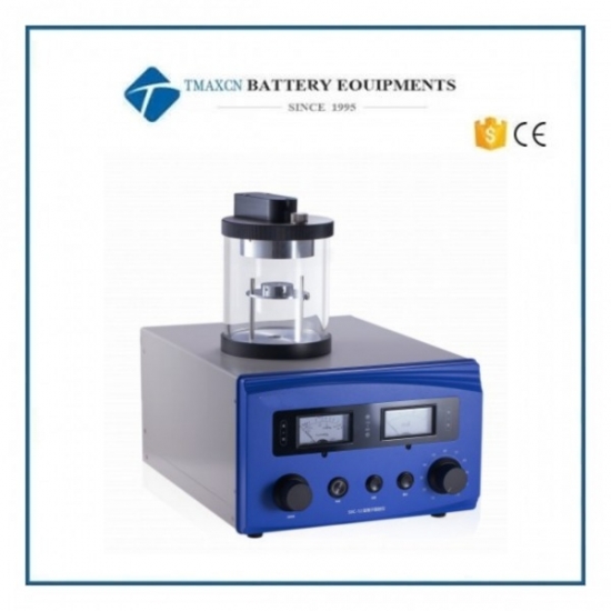
Nano Vacuum Magnetron Ion Sputtering Coater For Thin Film Fabrication
Model Number:
TMAX-ZK-JS05Input Power:
2000WCompliance:
CE CertifiedWarranty:
One Year limited warranty with lifetime supportShipping Port:
XiamenMOQ:
1Payment:
L/C D/A D/P T/T Western UnionDelivery Time:
5 days
- WhatsApp : +86 18659217588
- Email : David@tmaxcn.com
- Email : Davidtmaxcn@gmail.com
- Wechat : 18659217588
Previous:
Lab PVD Ion Sputtering Coater For Metal and Carbon LayerNext:
PVD Magnetron Sputter Coating System For SEM & Wafer Sample Preparation
Nano Vacuum Magnetron Ion Sputtering Coater For Thin Film Fabrication
Model: TMAX-ZK-JS05- Compact Ion Sputtering Coater
Overview
The TMAX-ZK-JS05 Compact Ion Sputtering Coater is designed for depositing conductive gold films on samples for scanning electron microscopy (SEM). With user-friendly operation, it is an essential tool for sample preparation in small to medium-sized SEM laboratories.
Key Applications
· Gold ion sputtering for SEM sample coating.
· Compatible with target materials: Au, Pt, Cr, Ag, Ti, Cu, Ni, Au-Pd alloy, etc.
Technical Specifications
Category |
Specification |
Chamber Material |
Glass |
Chamber Dimensions |
Ø100 mm (diameter) × 130 mm (height) |
Sample Stage (Small) |
Ø40 mm (holds 6 sample cups simultaneously) |
Sample Stage (Large, Optional) |
Ø60 mm |
Gold Target Size |
Ø58 mm |
Vacuum Pump |
Two-stage direct-drive rotary vane pump (1 L/s) |
Vacuum Measurement |
Pirani gauge |
Vacuum Protection |
20 Pa with fine-adjustment gas inlet valve |
Working Gases |
Air / Argon (dedicated inlet with flow control) |
Features & Advantages
· Robust Design – Special sealing structure minimizes glass chamber damage.
· High Compatibility – Supports Au, Pt, Cr, Ag, Ti, Cu, Ni, and Au-Pd alloy targets.
· Precision Control – Adjustable gas flow and vacuum protection ensure uniform coatings.
· Efficient Workflow – Dual-stage platform allows batch processing (6 samples at once).
Recommended Applications
✔ SEM Sample Prep – Ideal for non-conductive specimen coating.
✔ Materials Research – Thin-film deposition for nanotechnology studies.
✔ Industrial QC – Reliable performance for repeatable conductive layering.


 +86 13174506016
 David@tmaxcn.com

