 English▼


products categories
- Battery Production Equipment Line
- Battery Lab Pilot Equipment Line
- Lithium Battery Pack Assembly Line
- Solid State Battery Assembly Line
- Sodium Ion Battery Production Line
- Supercapacitor Assembly Line
- Lithium Ion Battery Recycling Plant
- Dry Electrode Preparation Solution
- Perovskite Based Solar Cell Lab Line
- Li ion Battery Materials
- Cathode Active Materials
- Anode Active Materials
- Customized Battery Electrode
- Coin Cell Parts
- Lithium Chip
- Cylindrical Cell Parts
- Battery Current Collectors
- Battery Conductive Materials
- Electrolyte
- Metal Mesh
- Battery Binder
- Separator and Tape
- Aluminum Laminate Film
- Nickel Strip
- Battery Tabs
- Graphene Materials
- Nickel Felt
- Titanium Fiber Felt
- Battery
- Battery Pack Machine & Compoments
- Battery Pack Compoments
- Turnkey Solutions Battery Pack Assembly Line
- Cell Sorter
- Battery Pack Spot Welder
- Laser Welder
- Battery Charging Discharging Tester
- Battery Pack Aging Machine
- Battery Pack Comprehensive Tester
- CCD Visual Inspector
- Battery Pape Sticking Machine
- BMS Testing Machine
- Al Wire Bonding Machine
- Lithium Battery Machine
- Battery Tester & Analyzer
- Battery Safety Tester
- Material Characterization Tester
- Rolling Press Machine
- Spot Welding Machine
- Vacuum Mixer Machine
- Crimping/Disassembling Machine
- Vacuum Sealing Machine
- Electrolyte Filling
- Stacking/Winding Machine
- Electrode Cutter/Slitter
- Pouch Forming Machine
- NMP Solvent Treatment System
- Lithium Battery Production Plant
- Vacuum Glove Box
- Furnaces
- Coaters
- PVD Coater
- Laboratory Press Machine
- Large Press Machine
- Planetary Centrifugal Mixer
- Ball Mill
- Laboratory Machine
- Cutting Machine
- Metal Foam
contact us
- If you have questions, please contact us, all questions will be answered
- WhatsApp : +86 18659217588
- Email : David@tmaxcn.com
- Email : Davidtmaxcn@gmail.com
- Add : No. 39, Xinchang Road, Xinyang, Haicang Dist., Xiamen, Fujian, China (Mainland)
RF Sputtering Coater System For Solar, OLED & Semiconductor
Model Number:
TMAX-PD-JS05Input Power:
2000WCompliance:
CE CertifiedWarranty:
One Year limited warranty with lifetime supportShipping Port:
XiamenMOQ:
1Payment:
L/C D/A D/P T/T Western UnionDelivery Time:
5 days
- WhatsApp : +86 18659217588
- Email : David@tmaxcn.com
- Email : Davidtmaxcn@gmail.com
- Wechat : 18659217588
Previous:
Multi-target Magnetron Sputtering Coating System For Multilayer Thin Film FabricationNext:
Multi-target Magnetron Sputtering Machine For Parylene,OLED, Solar Cell & Semiconductor
RF Sputtering Coater System For Solar, OLED & Semiconductor
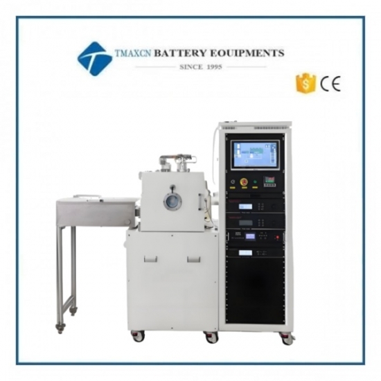
Model: TMAX-PD-JS05-Wafer Sputtering Coater System
Product Overview
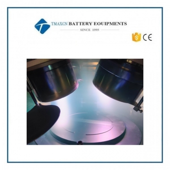
The TMAX-PD-JS05 magnetron sputtering system is equipped with multiple sputtering sources, capable of depositing metallic, semiconducting, and dielectric materials. It supports the fabrication of multilayer thin films and co-sputtered alloy films with high precision.
Key Features
· Compact & Integrated Design: Space-saving layout with refined aesthetics, optional sample-loading functionality.
· High Uniformity Coating: Features 4× magnetron sputtering targets (2–4 inches), compatible with 2–8 inch wafers. Substrate holder ensures uniformity within ±3%–5% for 8-inch wafers.
· Flexible Control Options: Siemens PLC + touchscreen (manual/automatic) or PC + PLC full-automatic control.
Technical Specifications
· System Dimensions (L×W×H): 1400 × 1300 × 1900 mm
· Chamber Dimensions (L×W×H): 500 × 500 × 500 mm (PD-500C) / 600 × 600 × 500 mm (PD-600C)
· Substrate Stage: Max heating temperature 500–800°C
· Base Pressure: ≤5 × 10⁻⁵ Pa
· Pumping & Holding: Achieves 8 × 10⁻⁴ Pa within ≤30 min; pressure rise ≤8 Pa over 12 hours.
· Target Configuration: 4× sputter guns (2–3 inches or 2–4 inches), coating area 2–6 inches.
Applications & Advantages
Ideal for R&D and small-batch production, the PD-500C/600C excels in depositing high-quality, uniform thin films for optics, electronics, and functional coatings. Its modular control and excellent temperature/vacuum stability cater to advanced material research and industrial precision demands.
TMAX-PD-JS05 vs. Conventional Model
Feature |
|
Conventional Systems |
Advantage |
Uniformity (8-inch wafer) |
±3%–5% |
±5%–10% or worse |
Higher film consistency for precision applications |
System Footprint |
Compact (1400×1300×1900 mm) |
30–50% larger |
Saves lab/cleanroom space |
Substrate Heating |
500–800°C |
Typically 300–600°C |
Supports high-temperature depositions (e.g., oxides, nitrides) |
Base Vacuum |
≤5×10⁻⁵ Pa |
~1×10⁻⁴ Pa |
Better for reactive sputtering, reduced contamination |
Pressure Stability |
≤8 Pa over 12 hours |
Frequent drift (>10 Pa in hours) |
Longer process stability |
Control Options |
PLC + Touchscreen or PC + PLC |
Manual or basic PLC |
Flexible automation, better reproducibility |
Target Configuration |
4× guns (2–4 inch) |
Often 2–3 guns (2–3 inch) |
Wider material selection, co-sputtering capability |
Coating Area |
2–8 inch wafers |
Typically ≤6 inch |
Broader substrate compatibility |
Key Takeaways
· Precision & Consistency: Superior uniformity (±3–5%) vs. conventional (±5–10%).
· Compact & Efficient: 30% smaller footprint without sacrificing performance.
· High-Temp & Vacuum Stability: Enables advanced materials (e.g., optical coatings, semiconductors).
· Automation Ready: PC-controlled processes improve repeatability over manual systems.
Ideal For: R&D labs, semiconductor fabs, and optical coating producers needing high-repeatability, multi-material deposition in a space-efficient design.


 +86 13174506016
 David@tmaxcn.com

