products categories
- Battery Production Equipment Line
- Battery Lab Pilot Equipment Line
- Lithium Battery Pack Assembly Line
- Solid State Battery Assembly Line
- Sodium Ion Battery Production Line
- Supercapacitor Assembly Line
- Lithium Ion Battery Recycling Plant
- Dry Electrode Preparation Solution
- Perovskite Based Solar Cell Lab Line
- Li ion Battery Materials
- Cathode Active Materials
- Anode Active Materials
- Customized Battery Electrode
- Coin Cell Parts
- Lithium Chip
- Cylindrical Cell Parts
- Battery Current Collectors
- Battery Conductive Materials
- Electrolyte
- Metal Mesh
- Battery Binder
- Separator and Tape
- Aluminum Laminate Film
- Nickel Strip
- Battery Tabs
- Graphene Materials
- Nickel Felt
- Titanium Fiber Felt
- Battery
- Battery Pack Machine & Compoments
- Battery Pack Compoments
- Turnkey Solutions Battery Pack Assembly Line
- Cell Sorter
- Battery Pack Spot Welder
- Laser Welder
- Battery Charging Discharging Tester
- Battery Pack Aging Machine
- Battery Pack Comprehensive Tester
- CCD Visual Inspector
- Battery Pape Sticking Machine
- BMS Testing Machine
- Al Wire Bonding Machine
- Lithium Battery Machine
- Battery Tester & Analyzer
- Battery Safety Tester
- Material Characterization Tester
- Rolling Press Machine
- Spot Welding Machine
- Vacuum Mixer Machine
- Crimping/Disassembling Machine
- Vacuum Sealing Machine
- Electrolyte Filling
- Stacking/Winding Machine
- Electrode Cutter/Slitter
- Pouch Forming Machine
- NMP Solvent Treatment System
- Lithium Battery Production Plant
- Vacuum Glove Box
- Furnaces
- Coaters
- PVD Coater
- Laboratory Press Machine
- Large Press Machine
- Planetary Centrifugal Mixer
- Ball Mill
- Laboratory Machine
- Cutting Machine
- Metal Foam
contact us
- If you have questions, please contact us, all questions will be answered
- WhatsApp : +86 18659217588
- Email : David@tmaxcn.com
- Email : Davidtmaxcn@gmail.com
- Add : No. 39, Xinchang Road, Xinyang, Haicang Dist., Xiamen, Fujian, China (Mainland)
Versatile Magnetron Sputtering Coater For Conductive Metal Thin Film Layer Deposition
Model Number:
TMAX-BY-JS05Input Power:
2000WCompliance:
CE CertifiedWarranty:
One Year limited warranty with lifetime supportShipping Port:
XiamenMOQ:
1Payment:
L/C D/A D/P T/T Western UnionDelivery Time:
5 days
- WhatsApp : +86 18659217588
- Email : David@tmaxcn.com
- Email : Davidtmaxcn@gmail.com
- Wechat : 18659217588
Previous:
High-Precision PVD Magnetron Sputtering & Thermal Evaporation Carbon Coating MachineNext:
Glovebox Dual-Target Sputtering Coating Machine Coater For Oxides & Ceramics & Semiconductors
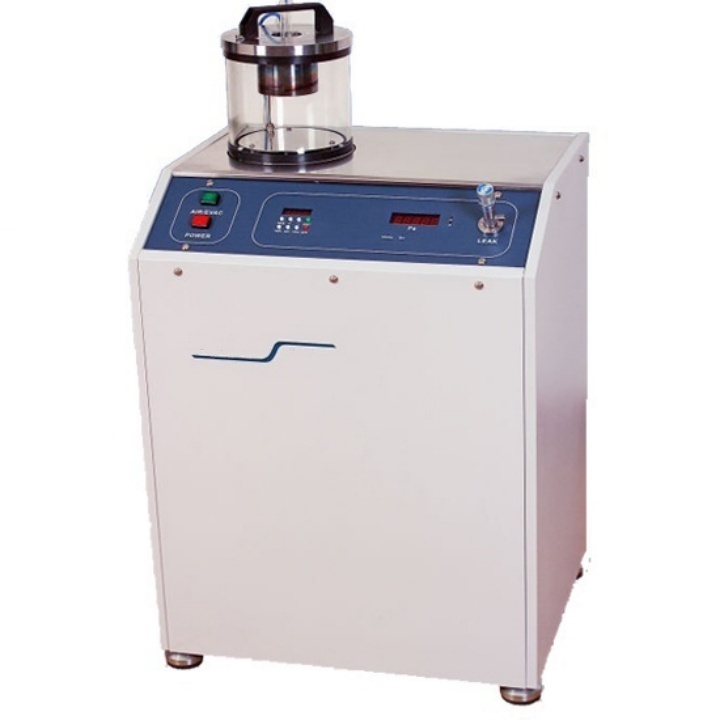
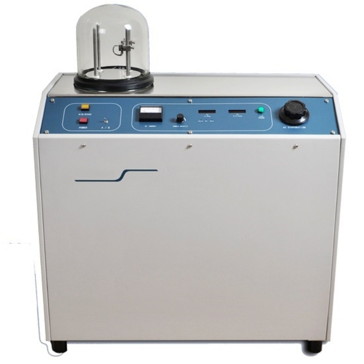
Versatile Magnetron Sputtering Coater For Conductive Metal Thin Film Layer Deposition
Model: TMAX-BY-JS06-Benchtop System for R&D and Educational Laboratories
Overview
The TMAX-BY-JS06 is a compact, cost-effective, high-vacuum magnetron sputtering system designed for pilot-scale experiments in research and educational laboratories. It integrates key components, including a sputtering vacuum chamber, permanent magnet targets (strong/weak magnetic fields), a fiber-optic rotary stage (customizable), DC power supply, gas supply system, pumping system, water cooling system, film thickness monitoring, vacuum measurement, electronic control system, and a sturdy mounting frame.
Key Parameters
Parameter |
Specification |
Sputtering Gas |
Adjustable (e.g., argon, nitrogen, etc., depending on experimental requirements). |
Target Material |
Standard: Gold target; Optional: Silver, copper, chromium, etc. |
Target Configuration |
50mm (weak magnetic target) / 60mm (strong magnetic target). |
Sputtering Current |
0–500mA |
Ultimate Vacuum |
≤5×10⁻⁴ Pa |
Chamber Dimensions |
Diameter: 180mm; Height: 200mm |
Sample Stage |
Fiber-optic rotary stage (customizable). |
Operating Voltage |
230V, 50Hz |
Applications & Features
1. Coating for Electron Beam-Sensitive Samples
· Ideal for: Biological specimens, polymers, and other beam-sensitive materials.
· Advantage: In SEM imaging, high-energy electron beams can cause thermal damage to delicate samples. A thin sputtered conductive coating (e.g., gold or carbon) acts as a protective layer, preserving sample integrity while enhancing imaging quality.
2. Non-Conductive Samples
· Ideal for: Insulating materials (e.g., ceramics, glass, or organic compounds).
· Advantage: Non-conductive samples accumulate surface charges ("charging effect") under electron beams, distorting SEM images. A sputtered conductive metal layer (e.g., gold or platinum) dissipates charges, eliminating artifacts and improving signal-to-noise ratio for clearer imaging.
3. Electrode Fabrication & Conductivity Studies
· Ideal for: Novel materials requiring conductive electrodes for electrical property analysis.
· Advantage: Enables precise deposition of thin conductive films for experimental electrode fabrication, facilitating studies on material conductivity.


 English▼


 +86 13174506016
 David@tmaxcn.com

