 English▼


products categories
- Battery Production Equipment Line
- Battery Lab Pilot Equipment Line
- Lithium Battery Pack Assembly Line
- Solid State Battery Assembly Line
- Sodium Ion Battery Production Line
- Supercapacitor Assembly Line
- Lithium Ion Battery Recycling Plant
- Dry Electrode Preparation Solution
- Perovskite Based Solar Cell Lab Line
- Li ion Battery Materials
- Cathode Active Materials
- Anode Active Materials
- Customized Battery Electrode
- Coin Cell Parts
- Lithium Chip
- Cylindrical Cell Parts
- Battery Current Collectors
- Battery Conductive Materials
- Electrolyte
- Metal Mesh
- Battery Binder
- Separator and Tape
- Aluminum Laminate Film
- Nickel Strip
- Battery Tabs
- Graphene Materials
- Nickel Felt
- Titanium Fiber Felt
- Battery
- Battery Pack Machine & Compoments
- Battery Pack Compoments
- Turnkey Solutions Battery Pack Assembly Line
- Cell Sorter
- Battery Pack Spot Welder
- Laser Welder
- Battery Charging Discharging Tester
- Battery Pack Aging Machine
- Battery Pack Comprehensive Tester
- CCD Visual Inspector
- Battery Pape Sticking Machine
- BMS Testing Machine
- Al Wire Bonding Machine
- Lithium Battery Machine
- Battery Tester & Analyzer
- Battery Safety Tester
- Material Characterization Tester
- Rolling Press Machine
- Spot Welding Machine
- Vacuum Mixer Machine
- Crimping/Disassembling Machine
- Vacuum Sealing Machine
- Electrolyte Filling
- Stacking/Winding Machine
- Electrode Cutter/Slitter
- Pouch Forming Machine
- NMP Solvent Treatment System
- Lithium Battery Production Plant
- Vacuum Glove Box
- Furnaces
- Coaters
- PVD Coater
- Laboratory Press Machine
- Large Press Machine
- Planetary Centrifugal Mixer
- Ball Mill
- Laboratory Machine
- Cutting Machine
- Metal Foam
contact us
- If you have questions, please contact us, all questions will be answered
- WhatsApp : +86 18659217588
- Email : David@tmaxcn.com
- Email : Davidtmaxcn@gmail.com
- Add : No. 39, Xinchang Road, Xinyang, Haicang Dist., Xiamen, Fujian, China (Mainland)
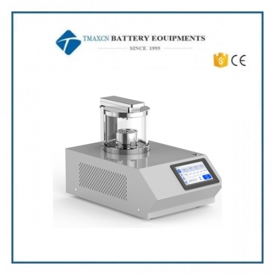
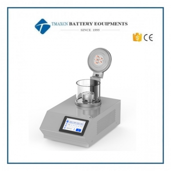
Magnetron Sputter Depostion Coater Machine PVD System For SEM
Model Number:
TMAX-HZ-JS03Input Power:
2000WCompliance:
CE CertifiedWarranty:
One Year limited warranty with lifetime supportShipping Port:
XiamenMOQ:
1Payment:
L/C D/A D/P T/T Western UnionDelivery Time:
5 days
- WhatsApp : +86 18659217588
- Email : David@tmaxcn.com
- Email : Davidtmaxcn@gmail.com
- Wechat : 18659217588
Previous:
Versatile Magnetron Sputtering System For Functional Metal Film Deposition CoatingNext:
High-Vacuum Dual-Target Magnetron Ion Sputtering Coating System Coater
Magnetron Sputter Depostion Coater Machine PVD System For SEM
Model: TMAX-HZ-JS03- Au/Carbon Coating Magnetron Sputter Coater
Product Overview
The TMAX-HZ-JS03 Dual-Target Magnetron Ion Sputtering Coater, independently developed with cutting-edge technology, sets a new benchmark for sample preparation instruments. It integrates dual-target co-sputtering and multi-layer single-sputtering capabilities, featuring a standard rotating/tilting module for multi-angle, uniform film coverage. This design eliminates charging effects, enhances sample contrast, and delivers high-resolution, true-to-life morphological characterization—ideal for advanced material science and biological research.
Technical Specifications
Category |
Parameter |
Specification |
Core Parameters |
Model |
TMAX-HZ-JS03 |
|
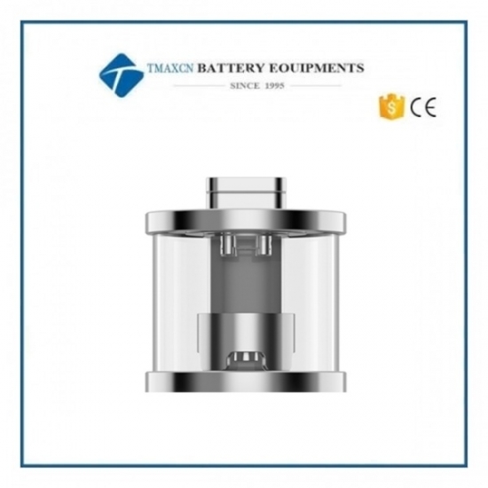
Vacuum Chamber (mm) |
160 × 120 |
|
Sputtering Voltage |
300–700 V |
|
Sample Stage (mm) |
Adjustable 80–100 diameter |
|
Sputtering Type |
Magnetron |
|
Working Vacuum |
2–10 Pa |
System Configuration |
Power Supply |
100–250 VAC, 50/60 Hz |
|
Target Size (mm) |
φ50 × 0.1 |
|
Control System |
5" Touchscreen (ARM) |
|
Max. Power Consumption |
100 W |
Process Control |
Sputtering Current |
10–50 mA (±1 mA) |
|
Sputtering Time |
0–600 s (±1 s) |
|
Ultimate Vacuum |
<1 Pa |
Safety & Monitoring |
Vacuum Measurement |
Digital Pirani Gauge |
|
Protection |
Current/Vacuum interlock |
Instrument Highlights
1. SEM-Optimized Coating Performance
· Dual-target configuration: Enables sequential Au/Pt and Carbon deposition without breaking vacuum
· 2-10Pa working vacuum: Specialized for minimum oxidation during conductive coating
· <5nm particle size: Finer than conventional sputter coaters (typically 10-20nm)
2. Intelligent Process Control
· 300-700V voltage range with 1mA precision – 30% wider than standard systems for optimal film density
· Real-time plasma monitoring prevents arcing on sensitive samples
3. Ergonomic Design
· 160mm large chamber: Accommodates tall SEM stubs (up to 25mm) and irregular specimens
· Tool-free target change
Target Applications
▸ Life Science: Coating for pollen, plant tissues, and hydrated biological samples
▸ Materials Research: Nanowires, polymer films, and porous materials
▸ Failure Analysis: PCB cross-sections and insulating components
Operational Advantages
· One-cycle coating: 12 samples/batch (50% more than competitors)
· Zero thermal damage: Magnetron confinement keeps samples <40°C
· Self-diagnostics: Automatic pump protection and target life counter


 +86 13174506016
 David@tmaxcn.com

