 English▼


products categories
- Battery Production Equipment Line
- Battery Lab Pilot Equipment Line
- Lithium Battery Pack Assembly Line
- Solid State Battery Assembly Line
- Sodium Ion Battery Production Line
- Supercapacitor Assembly Line
- Lithium Ion Battery Recycling Plant
- Dry Electrode Preparation Solution
- Perovskite Based Solar Cell Lab Line
- Li ion Battery Materials
- Cathode Active Materials
- Anode Active Materials
- Customized Battery Electrode
- Coin Cell Parts
- Lithium Chip
- Cylindrical Cell Parts
- Battery Current Collectors
- Battery Conductive Materials
- Electrolyte
- Metal Mesh
- Battery Binder
- Separator and Tape
- Aluminum Laminate Film
- Nickel Strip
- Battery Tabs
- Graphene Materials
- Nickel Felt
- Titanium Fiber Felt
- Battery
- Battery Pack Machine & Compoments
- Battery Pack Compoments
- Turnkey Solutions Battery Pack Assembly Line
- Cell Sorter
- Battery Pack Spot Welder
- Laser Welder
- Battery Charging Discharging Tester
- Battery Pack Aging Machine
- Battery Pack Comprehensive Tester
- CCD Visual Inspector
- Battery Pape Sticking Machine
- BMS Testing Machine
- Al Wire Bonding Machine
- Lithium Battery Machine
- Battery Tester & Analyzer
- Battery Safety Tester
- Material Characterization Tester
- Rolling Press Machine
- Spot Welding Machine
- Vacuum Mixer Machine
- Crimping/Disassembling Machine
- Vacuum Sealing Machine
- Electrolyte Filling
- Stacking/Winding Machine
- Electrode Cutter/Slitter
- Pouch Forming Machine
- NMP Solvent Treatment System
- Lithium Battery Production Plant
- Vacuum Glove Box
- Furnaces
- Coaters
- PVD Coater
- Laboratory Press Machine
- Large Press Machine
- Planetary Centrifugal Mixer
- Ball Mill
- Laboratory Machine
- Cutting Machine
- Metal Foam
contact us
- If you have questions, please contact us, all questions will be answered
- WhatsApp : +86 18659217588
- Email : David@tmaxcn.com
- Email : Davidtmaxcn@gmail.com
- Add : No. 39, Xinchang Road, Xinyang, Haicang Dist., Xiamen, Fujian, China (Mainland)
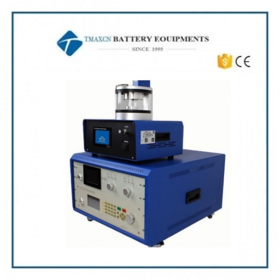
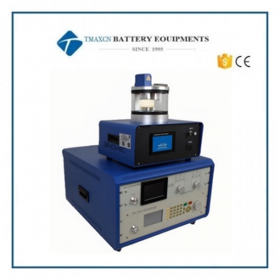
RF Magnetron Sputtering System for Metals & Non-Metals Film Deposition
Model Number:
TMAX-SD-JS01Input Power:
2000WCompliance:
CE CertifiedWarranty:
One Year limited warranty with lifetime supportShipping Port:
XiamenMOQ:
1Payment:
L/C D/A D/P T/T Western UnionDelivery Time:
5 days
- WhatsApp : +86 18659217588
- Email : David@tmaxcn.com
- Email : Davidtmaxcn@gmail.com
- Wechat : 18659217588
Previous:
PVD Magnetron Sputtering System For Thin Film Deposition In Research, Semiconductor Prototyping and Optical CoatingNext:
Magnetron Ion Thermal Evaporation Carbon Sputter Coater for SEM Sample Preparation
RF Magnetron Sputtering System for Metals & Non-Metals Film Deposition
Model: TMAX-SD-01-Metals & Non-Metals: Insulators, Semiconductors, Carbon-Based Thin Film Deposition
Product Specifications
Parameter |
Specification |
Model |
TMAX-SD-01 |
Type |
RF Magnetron Sputtering System |
Chamber Size |
150 × 120 mm |
Target Material |
50 mm diameter (metals & non-metals, thickness: 1–2 mm) |
RF Power |
Adjustable (1–500 W) |
RF Frequency |
13.56 MHz |
Matching Network |
Automatic impedance matcher |
Sputtering Area |
50 mm |
Ultimate Vacuum |
5 Pa (base pressure) |
Process Gases |
Argon, nitrogen, and other inert gases (flow rate adjustable) |
Max. Deposition Rate |
8 nm/min |
Key Features & Applications
1. Versatile RF Sputtering for Metals & Non-Metals
· RF Power & Auto-Matching: 13.56 MHz RF with automatic impedance matching ensures stable sputtering of both conductive and insulating materials (e.g., oxides, ceramics).
· Broad Applications: Ideal for advanced thin-film research in semiconductors, optics, and functional coatings.
2. Precise Gas Control & High Vacuum Performance
· Adjustable Inert Gas Flow: Supports Ar, N₂, and other inert gases for controlled deposition environments.
· High Purity Deposition: Base vacuum of 5 Pa minimizes contamination, ensuring high-quality film growth.
3. User-Friendly & Efficient Operation
· Quick Target Change: Compatible with 50 mm targets (1–2 mm thick) for flexible material testing.
· Preset Process Recipes: Saves and recalls parameters for repeatable experiments and production.
4. Stable & High-Speed Deposition
· Max Deposition Rate: 8 nm/min with excellent film uniformity.
· Automated Matching: Reduces manual tuning and enhances process stability.
Recommended Applications
✔ Research & Development: Thin-film studies for semiconductors, dielectrics, and optical coatings.
✔ Small-Scale Production: Prototyping and specialized coating applications.
✔ Multi-Material Sputtering: Supports both metallic and non-metallic targets for diverse material systems.


 +86 13174506016
 David@tmaxcn.com

